LeapSecond.com
picDIV -- Single Chip Frequency Divider
20-Oct-2011
Introduction
There are many ways to divide frequency.
If the frequency is 10 MHz and the desired frequency is 1 Hz,
one needs to divide by 10 million.
This is easily accomplished with a series of discrete decade counters.
But a tiny microcontroller can perform the same function.
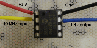
 picDIV™ is a PIC-based digital frequency divider
that functions like a series of synchronous decade counters.
As seen here,
a "PIC" is a ubiquitous, tiny, inexpensive, 8-bit microcontroller.
A simple software program "spins" and every 5 million
clock cycles the CPU toggles the output pin.
Thus a 10 MHz input clock signal becomes a 1 Hz square wave output.
picDIV™ is a PIC-based digital frequency divider
that functions like a series of synchronous decade counters.
As seen here,
a "PIC" is a ubiquitous, tiny, inexpensive, 8-bit microcontroller.
A simple software program "spins" and every 5 million
clock cycles the CPU toggles the output pin.
Thus a 10 MHz input clock signal becomes a 1 Hz square wave output.
Output accuracy is equal to input accuracy.
Jitter is extremely low since the PIC is a synchronous device.
Recent measurement suggest it is less than 2 ps.
Operation
A picDIV chip could not be simpler to use.
Besides +5 VDC power (pin 1) and ground (pin 8) there are only two pins!
 pin 2 -- The 10 MHz clock drives the PIC (it runs isochronous code).
A CMOS-compatible square wave is ideal
but the PIC clock input is rather forgiving.
For example, if the level and amplitude is appropriate even a 10 MHz sinewave will work.
pin 2 -- The 10 MHz clock drives the PIC (it runs isochronous code).
A CMOS-compatible square wave is ideal
but the PIC clock input is rather forgiving.
For example, if the level and amplitude is appropriate even a 10 MHz sinewave will work.
pin 7 -- The 1 Hz square wave output.
Variations
When a programmable synchronous microcontroller is clocked from an accurate frequency reference,
many interesting, practical, one-chip solutions come to mind.
The initial 10 MHz to 1 Hz divider evolved into dozens of useful devices.
Powers of ten dividers
- PD3 divides by one thousand (103),
e.g., 10 MHz→10 kHz
- PD4 divides by ten thousand (104),
e.g., 10 MHz→1 kHz
- PD5 divides by hundred thousand (105),
e.g., 10 MHz→100 Hz
- PD6 divides by one million (106),
e.g., 10 MHz→10 Hz or 1 MHz→1 Hz
- PD7 divides by ten million (107),
e.g., 10 MHz→1 Hz
- PD8 divides by five million,
e.g., 5 MHz→1 Hz
Note: there is no requirement to always drive these dividers with 10 MHz.
A PD3 will divide by 1000 regardless of the input frequency;
the output frequency is always 1000 times less than the input.
The PIC clock operates from DC to 20 MHz.
Narrow pulse outputs
The following picDIV dividers output narrow pulses instead of a 50% square wave.
- PD9 generates 1PPS from 10 MHz.
The output is a very narrow 20 µs pulse,
which is more than enough to trigger counter instruments
and small enough to have near zero average power.
- PD10 generates 1PPS from 10 MHz.
The output is a 10 ms pulse,
which is just long enough for a visible heartbeat LED.
Connection diagram for PD7 (and PD3, PD4, PD5, PD6, PD8, PD9, PD10)
                             ---__---
             5V (Vdd)  +++++|1      8|=====  Ground (Vss)
          input clock  ---->|2  pD  7|---->  output clock
                           *|3  07  6|*
                           o|4      5|o
                             --------
Note: For PD3 through PD10, pin 3 and pin 6 are outputs along with pin 7.
This can be useful if multiple outputs or higher current (parallel drive) is desired.
On these chips, pin 4 and pin 5 are not used and may be be left open or tied to Vdd or Vss.
Synchronized dividers
The following 1PPS dividers have multiple output widths and 1PPS sync capability.
- PD11 takes a 10 MHz clock
and generates three different 1 Hz outputs:
a narrow 100 µs pulse is output from pin 7,
a 10 ms pulse is output from pin 3, and
a 1 Hz square wave is output from pin 6.
- PD12 takes a 5 MHz clock
and generates three different 1 Hz outputs:
a narrow 100 µs pulse is output from pin 7,
a 10 ms pulse is output from pin 3, and
a 1 Hz square wave is output from pin 6.
The narrow pulse is good for triggering time interval or frequency counters,
and long enough for use with PC serial ports.
The 10 ms pulse is convenient for blinking a LED.
These dividers also allow for 1PPS synchronization.
If pin 4 (Arm) is held low for a second the divider stops and waits.
The divider synchronizes to the rising edge of pin 5 (Sync).
There is a weak pullup on the Sync pin.
If you never plan to stop or sync the divider connect the Arm pin to Vdd,
or simply connect the Arm pin to the Sync pin.
Connection diagram for PD11:
                             ---__---
             5V (Vdd)  +++++|1      8|=====  Ground (Vss)
      10 MHz clock in  ---->|2  pD  7|---->  1PPS out (100 us)
     1PPS (10 ms) out  <----|3  11  6|---->  1 Hz out (50%)
                  Arm  o--->|4      5|<+---  Sync
                             --------
Connection diagram for PD12:
                             ---__---
             5V (Vdd)  +++++|1      8|=====  Ground (Vss)
       5 MHz clock in  ---->|2  pD  7|---->  1PPS out (100 us)
     1PPS (10 ms) out  <----|3  12  6|---->  1 Hz out (50%)
                  Arm  o--->|4      5|<+---  Sync
                             --------
Observe that if all you need is the 100 µs output this is a 4-pin IC.
If you want all three outputs it is a "6-pin IC".
If you want synchronization it is a full "8-pin" IC.
Multiple output frequencies
Several dividers have been designed with multiple square wave frequency outputs,
from 1 Hz to 10 kHz.
- PD13 (10 MHz input clock) generates three outputs:
1 Hz, 10 Hz, 100 Hz, with optional Arm/Sync.
- PD14 (5 MHz input clock) generates three outputs:
1 Hz, 10 Hz, 100 Hz, with optional Arm/Sync.
- PD15 (10 MHz input clock) generates three outputs:
1 Hz, 1000 Hz, 10,000 Hz, with optional Arm/Sync.
Connection diagram for PD13:
                             ---__---
             5V (Vdd)  +++++|1      8|=====  Ground (Vss)
      10 MHz clock in  ---->|2  pD  7|---->  100 Hz out
             1 Hz out  <----|3  13  6|---->  10 Hz out
                  Arm  o--->|4      5|<+---  Sync
                             --------
Connection diagram for PD14:
                            ---__---
             5V (Vdd)  +++++|1      8|=====  Ground (Vss)
       5 MHz clock in  ---->|2  pD  7|---->  100 Hz out
             1 Hz out  <----|3  14  6|---->  10 Hz out
                  Arm  o--->|4      5|<+---  Sync
                             --------
Connection diagram for PD15:
                             ---__---
             5V (Vdd)  +++++|1      8|=====  Ground (Vss)
      10 MHz clock in  ---->|2  pD  7|---->  10 kHz out
             1 Hz out  <----|3  15  6|---->  1 kHz out
                  Arm  o--->|4      5|<+---  Sync
                             --------
Multiple input frequencies
Most frequency references today are 10 MHz,
but it is not rare to find 1.0 MHz, 2.5 MHz, or 5.0 MHz.
Several divider chips have been designed to accomodate this set of frequencies.
- PD16 (5 or 10 MHz input clock) generates four outputs:
1 Hz, 10 Hz, 100 Hz, 1000 Hz.
- PD17 (1, 2.5, 5, or 10 MHz) input clock generates one 1PPS output
(10% duty cycle), with optional Arm/Sync.
- PD18 (1, 2.5, 5, or 10 MHz) input clock generates one 1PPS output
(1% duty cycle), with optional Arm/Sync.
Connection diagram for PD16:
                             ---__---
             5V (Vdd)  +++++|1      8|=====  Ground (Vss)
    5/10 MHz clock in  ---->|2  pD  7|---->  1000 Hz out
             1 Hz out  <----|3  16  6|---->  100 Hz out
               Select  o--->|4      5|---->  10 Hz out
                             --------
Connection diagram for PD17:
                             ---__---
             5V (Vdd)  +++++|1      8|=====  Ground (Vss)
       N MHz clock in  ---->|2  pD  7|<+---  ConfigA
    1PPS (100 ms) out  <----|3  17  6|<+---  ConfigB
                  Arm  o--->|4      5|<+---  Sync
                             --------
Connection diagram for PD18:
                             ---__---
             5V (Vdd)  +++++|1      8|=====  Ground (Vss)
       N MHz clock in  ---->|2  pD  7|<+---  ConfigA
     1PPS (10 ms) out  <----|3  18  6|<+---  ConfigB
                  Arm  o--->|4      5|<+---  Sync
                             --------
Interface notes
- A bypass capacitor (e.g., 0.1 µF) is recommended between pin 1 and pin 8.
- A PIC output pin will drive 20 mA.
- Inputs are typically CMOS/TTL compatible signal levels.
- For some applications you may need to condition the input signal
or buffer the output signal.
Obviously this adds additional active and passive components to the solution.
On the other hand, for many applications no additional parts are required
and the picDIV chip is truely a one part solution.
- Output jitter is less than 2 ps.
- These PIC's will work from 2.0 to 5.5 V.
Availability
The relativity kids
have grown up a bit since you last saw them in 2005.
It's time for them to learn what work is.
I've assigned them the task of
taking orders, burning firmware, making labels, testing, packaging and shipping.
The cost is minimal:
- one picDIV is $3 (ten for $25, any combination)
- one picPET is $5 (ten for $40)
- first-class postage & handling is $4 (USA) or $8 (international)
- contact me (tvb@LeapSecond.com) for PayPal payments
Source Code
The kids are happy to make and deliver these chips for you.
But if you have the equipment and want to burn your own,
then click on the hex files or source code links given below.
Or maybe you just want to learn how the dividers work;
to see how simple it is to use microcontroller assembly language
to implement digital frequency division.
- pd03.asm / pd03.hex /
PD03 -- "4-pin" 10^3 frequency divider (10 MHz to 10 kHz)
- pd04.asm / pd04.hex /
PD04 -- "4-pin" 10^4 frequency divider (10 MHz to 1 kHz)
- pd05.asm / pd05.hex /
PD05 -- "4-pin" 10^5 frequency divider (10 MHz to 100 Hz)
- pd06.asm / pd06.hex /
PD06 -- "4-pin" 10^6 frequency divider (10 MHz to 10 Hz)
- pd07.asm / pd07.hex /
PD07 -- "4-pin" 10^7 frequency divider (10 MHz to 1 Hz)
- pd08.asm / pd08.hex /
PD08 -- "4-pin" 5x10^6 frequency divider (5 MHz to 1 Hz)
- pd09.asm / pd09.hex /
PD09 -- "4-pin" 10 MHz to 1PPS frequency divider (20 us pulse)
- pd10.asm / pd10.hex /
PD10 -- "4-pin" 10 MHz to 1PPS frequency divider (10 ms pulse)
- pd11.asm / pd11.hex /
PD11 -- 10 MHz to 1PPS frequency divider (3 pulse widths), with sync
- pd12.asm / pd12.hex /
PD12 -- 5 MHz to 1PPS frequency divider (3 pulse widths), with sync
- pd13.asm / pd13.hex /
PD13 -- 10 MHz to three frequencies divider (1-10-100 Hz), with sync
- pd14.asm / pd14.hex /
PD14 -- 5 MHz to three frequencies divider (1-10-100 Hz), with sync
- pd15.asm / pd15.hex /
PD15 -- 10 MHz to three frequencies divider (1-1000-10000 Hz), with sync
- pd16.asm / pd16.hex /
PD16 -- 5/10 MHz to four frequencies divider (1-10-100-1000 Hz)
- pd17.asm / pd17.hex /
PD17 -- 1/2.5/5/10 MHz to 1PPS frequency divider (100 ms), with sync
- pd18.asm / pd18.hex /
PD18 -- 1/2.5/5/10 MHz to 1PPS frequency divider (10 ms), with sync
- pd26.asm / pd26.hex /
PD26 -- 10 MHz to 1PPS divider, with sync and micro-step
- pd27.asm / pd27.hex /
PD27 -- 10 MHz to 1PPS divider, with sync and milli-step
- pd28.asm / pd28.hex /
PD28 -- 10 MHz to sidereal 1PPS divider, with sync and milli-step
If you have requests for special features, let me know.
See LeapSecond.com PIC project page.
Return to LeapSecond.com home page.
Comments/questions to tvb.